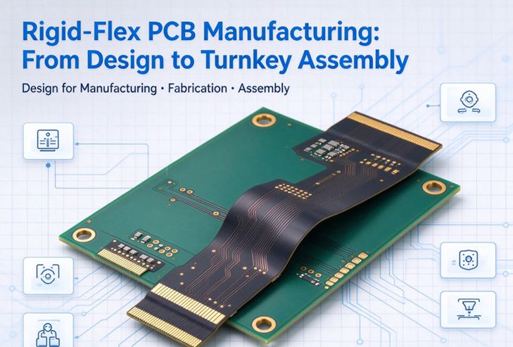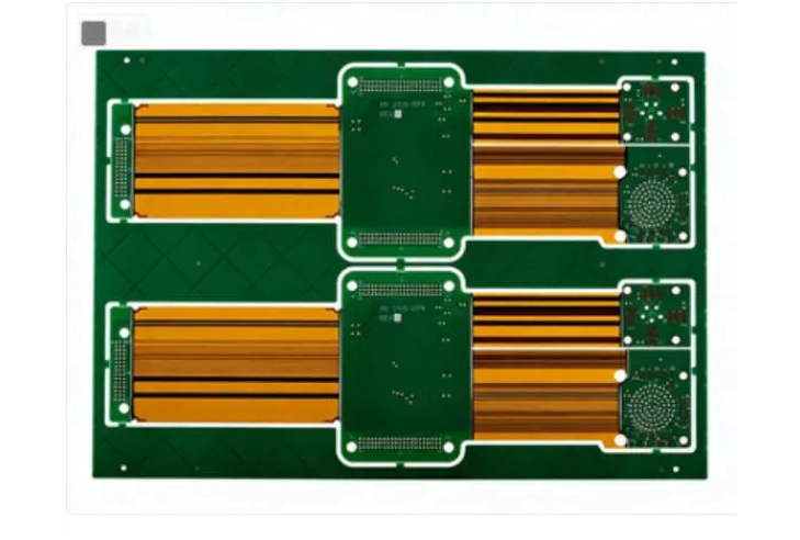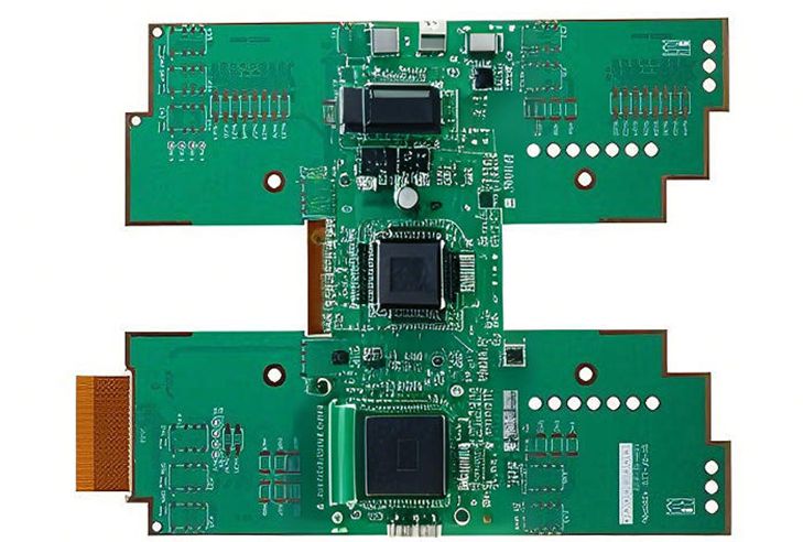
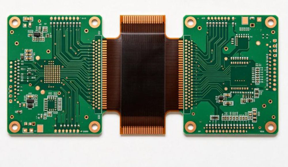
As electronic hardware keeps trending toward miniaturization, lightweight design and high integration, rigid‑flex PCB has transformed from niche specialty component to mainstream choice for many OEM and ODM projects. Global market data shows rigid‑flex PCB market will keep steady growth through 2031, driven by medical devices, industrial automation, automotive electronics and wearable equipment. Unlike standard rigid PCB or pure flexible circuit, rigid‑flex boards merge rigid FR‑4 sections and polyimide flexible layers within one single unit, removing bulky connectors and internal wiring harnesses while improving mechanical shock resistance.
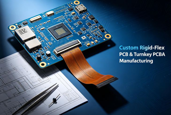
Core Benefits of Rigid‑Flex PCB for Hardware Developers
First of all, rigid‑flex structures reduce overall system size and weight. By eliminating multiple connectors and interconnection cables, designers can cut device assembly volume by 25‑30% in many compact products. In addition, fewer connectors mean fewer potential failure points. Vibration, thermal cycling and repeated bending will not easily break electrical contact, which is highly valuable for field‑deployed industrial and medical hardware.
Furthermore, signal integrity gets improved. Traditional multi‑board connection via cables introduces impedance discontinuity and signal loss. Rigid‑flex PCB creates continuous signal traces across rigid and flexible zones, delivering stable performance for high‑speed signal circuits. Even so, many project teams underestimate manufacturing complexity and run into delays during prototype or mass‑production phases.
Key Real‑World Challenges Facing Rigid‑‑Flex PCB Manufacturing
Even with obvious advantages, rigid‑flex PCB manufacturing brings unique pain points for procurement teams. Material mismatch represents one major obstacle. Rigid FR‑4 and polyimide flex substrates feature different thermal expansion coefficients. During lamination and reflow soldering, internal stress may trigger delamination, copper trace cracking or layer separation if stack‑up design is not well‑managed.
Besides material risks, bend‑zone layout is another frequent source of defects. Placing vias, pads or components inside bending areas will quickly lead to trace fracture after repeated flex cycles. Many generic PCB manufacturers do not hold enough experience to review rigid‑flex stack‑up, bend radius rules and material selection in early DFM phase, which leads to costly redesign after prototype production. Lead‑time pressure also adds difficulty: rigid‑flex prototype normally takes longer turnaround compared with ordinary rigid PCB due to complex multi‑step lamination workflow.
Early DFM Review Reduces Project Risks
For B‑side buyers, the most effective practice is to involve your PCB manufacturer in the schematic and layout stage. Experienced fabricators can check stack‑up configuration, bend area clearance, material grade and minimum bend radius before Gerber files are finalized. This collaborative review can avoid expensive redesign and shorten overall project timeline.
Working with an experienced in‑house manufacturer matters greatly for rigid‑flex projects. Ring PCB has accumulated rich know‑how in rigid‑flex PCB manufacturing, supporting custom stack‑up design, strict IPC‑6013 compliance, prototype validation and batch production. Our internal DFM team will examine every critical detail of your rigid‑flex design before production starts, helping customers mitigate typical flex‑rigid manufacturing pitfalls.
If you have ongoing rigid‑flex PCB projects requiring professional manufacturing support, please send your requirements to rfq@ringpcb.com.