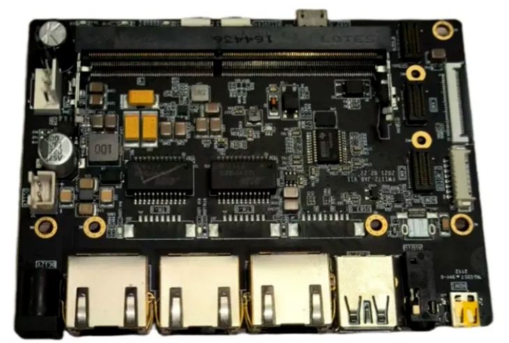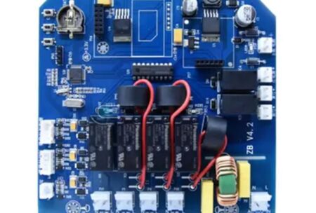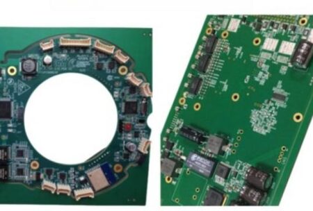

Multilayer PCB manufacturing allows electronic products to integrate complex signal routing, power distribution, and dense interconnections within compact circuit boards. These capabilities are essential for industrial controllers, communication equipment, power electronics, and embedded computing systems.
However, increasing PCB complexity also introduces manufacturing risks that cannot always be identified through surface inspection.
A finished board may look acceptable while containing weaknesses in plated through-holes, internal copper connections, or laminated dielectric materials.
Such defects can affect long-term reliability, particularly when electronic products experience repeated thermal cycling or continuous operation.
Therefore, OEM engineers should evaluate multilayer PCB manufacturing quality beyond appearance and initial electrical continuity.
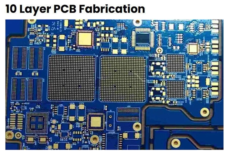
Why Internal PCB Reliability Matters
A multilayer PCB consists of conductive copper layers separated by insulating materials.
Electrical connections between layers depend on accurately drilled and plated holes, while structural stability depends on controlled lamination.
During assembly and operation, these materials experience thermal and mechanical stress.
For example, an industrial controller may operate through repeated heating and cooling cycles.
A communication module may remain powered continuously for extended periods.
If internal connections are weak, failures may appear only after the product has entered service.
Consequently, reliability requirements should be considered during manufacturing preparation rather than after defects occur.
Understand Plated Through-Hole Reliability
Plated through-holes establish electrical connections between different PCB layers.
Their performance depends on drilling accuracy, hole-wall preparation, copper deposition, and electroplating quality.
Poor hole-wall preparation can affect copper adhesion, while insufficient plating may create weak conductive structures.
These defects can contribute to intermittent electrical failures under thermal stress.
PCB thickness, finished hole diameter, aspect ratio, and copper requirements also influence manufacturing feasibility.
For OEMs, the practical approach is to provide complete drilling specifications and confirm the manufacturer’s applicable process capabilities.
Engineering review is particularly important for thick multilayer boards and designs with demanding via structures.
Prevent Lamination Defects
Lamination bonds individual PCB layers into a stable structure.
The process requires appropriate materials, temperature, pressure, and manufacturing controls.
Improper processing can contribute to delamination, voids, or internal structural defects.
Material selection is equally important.
Different laminates offer different glass transition temperatures, thermal expansion characteristics, and dielectric properties.
A material suitable for a standard industrial controller may not meet the requirements of a high-speed communication board.
Therefore, engineers should specify the intended material properties and operating conditions.
Manufacturers can then evaluate whether the selected construction is appropriate for fabrication and subsequent assembly.
Maintain Accurate Inner-Layer Registration
Accurate alignment between internal copper layers is essential for multilayer PCB manufacturing.
Registration errors may reduce annular ring dimensions or affect the relationship between drilled holes and internal conductors.
These problems become more critical as circuit density increases.
Manufacturing controls include inner-layer imaging, alignment, lamination registration, and drilling accuracy.
For high-density boards, tighter design rules may require additional process evaluation.
OEMs should identify critical tolerances and provide consistent fabrication data.
Furthermore, manufacturing adjustments that affect approved electrical or mechanical requirements should be reviewed before production.
Consider Thermal Stress During PCB Assembly
A multilayer PCB experiences thermal exposure during fabrication and assembly.
Reflow soldering, through-hole soldering, and repeated heating cycles can introduce additional stress.
Because copper and dielectric materials expand differently, temperature changes may place mechanical stress on plated holes and internal connections.
A weak connection may pass an initial electrical test but deteriorate after repeated thermal exposure.
For this reason, high-reliability applications may require additional qualification or thermal-stress testing.
The appropriate methods depend on product requirements and applicable standards.
Manufacturers should not assume that a standard electrical test demonstrates every aspect of long-term reliability.
Control Impedance in High-Speed Multilayer PCBs
High-speed communication equipment often requires controlled-impedance PCB structures.
Impedance depends on trace geometry, dielectric thickness, copper characteristics, and laminate properties.
Manufacturing variation can therefore affect electrical performance.
For example, an Ethernet or high-speed data interface may require defined single-ended or differential impedance values.
Engineers should provide target values, relevant structures, and acceptable tolerances.
The PCB manufacturer can then review stackup feasibility and manufacturing controls.
Ring PCB supports multilayer PCB fabrication and controlled-impedance manufacturing requirements, helping customers coordinate electrical specifications with practical fabrication processes.
Any proposed adjustment should remain subject to customer engineering approval.
Combine Electrical Testing With Structural Inspection
Bare-board electrical testing helps identify open and short circuits.
Flying probe testing is commonly used for prototype and lower-volume production, while fixture-based testing may be appropriate for larger quantities.
However, electrical continuity alone cannot reveal every internal structural weakness.
Microsection analysis can provide information about plated-hole construction, copper thickness, and selected internal features.
Visual inspection and dimensional verification provide additional evidence of manufacturing quality.
These methods address different risks and should be selected according to the product specification.
For demanding applications, OEMs should confirm inspection scope before placing the manufacturing order.

Use International Standards to Define Acceptance
International standards help PCB manufacturers and OEM customers establish consistent quality expectations.
IPC-6012F addresses qualification and performance requirements for rigid printed boards, while IPC-A-600 provides printed-board acceptability criteria.
However, the applicable performance class and additional acceptance requirements must be defined for each project.
Ring PCB reports UL, ISO 9001, ISO 14001, ISO 13485, and IATF 16949 certifications as part of its broader management and quality framework.
These credentials support structured manufacturing management, environmental responsibility, and specialized industry requirements.
Nevertheless, management-system certification should not be confused with product-specific approval or evidence that every board has undergone every possible reliability test.
Clear customer specifications remain essential.
Balance Reliability With Manufacturing Speed
Rapid production is valuable when OEMs need engineering samples or urgent manufacturing support.
Ring PCB offers PCB prototyping in as little as 3 days and qualifying PCB and PCBA production schedules as short as 7 days.
However, multilayer PCB turnaround depends on layer count, material availability, drilling complexity, impedance requirements, and inspection scope.
A specialized high-layer-count board may require different processing time from a conventional multilayer FR-4 design.
Therefore, manufacturers should evaluate the actual design before confirming a delivery schedule.
Speed should complement manufacturing quality, not replace necessary process controls.
What OEMs Should Confirm Before Ordering
A complete multilayer PCB request should include Gerber files, drill data, layer stackup, board thickness, copper requirements, material specifications, and surface finish.
If controlled impedance is required, engineers should identify target values and tolerances.
Critical mechanical requirements and inspection expectations should also be documented.
For products intended for demanding environments, the customer should communicate relevant reliability requirements.
This information allows the manufacturer to evaluate technical feasibility and prepare a more accurate quotation.
It also reduces the risk of misunderstanding between engineering and purchasing teams.
Multilayer PCB Manufacturing With Ring PCB
Reliable multilayer PCB manufacturing requires coordinated engineering review, controlled fabrication, and appropriate inspection.
Ring PCB provides custom multilayer PCB manufacturing, PCB prototyping, controlled-impedance fabrication, component sourcing, SMT and through-hole assembly, and full-turnkey PCBA services.
These capabilities support OEM customers developing industrial electronics, communication equipment, embedded devices, and other specialized products.
By coordinating fabrication requirements with downstream assembly needs, Ring PCB helps customers prepare projects for prototype validation and repeat manufacturing.
Send your Gerber files, stackup specifications, material requirements, quantities, and target schedule to rfq@ringpcb.com for project-specific review.
References
- IPC. IPC-6012F, Qualification and Performance Specification for Rigid Printed Boards.
- IPC. IPC-A-600, Acceptability of Printed Boards.
- Global Electronics Association. North American PCB Shipments Jump 23.5% in August, Extending Strong 2026 Growth. September 2026.
- Ring PCB. https://www.ringpcb.com/