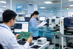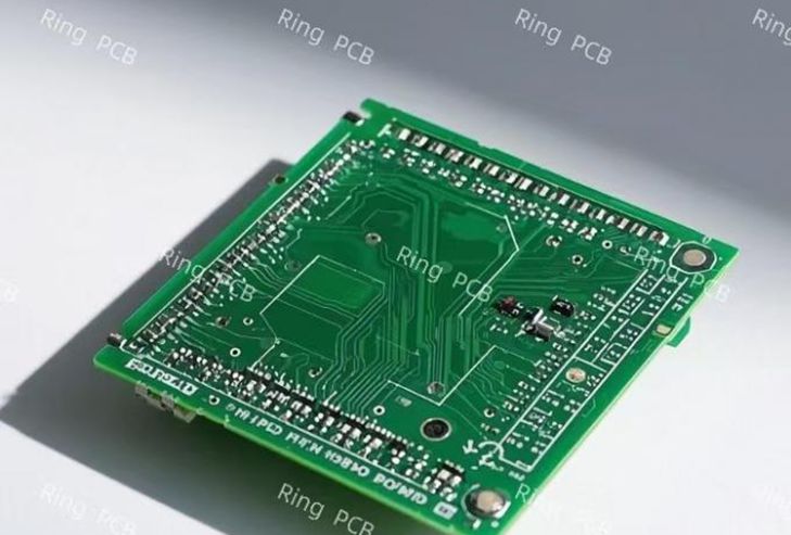
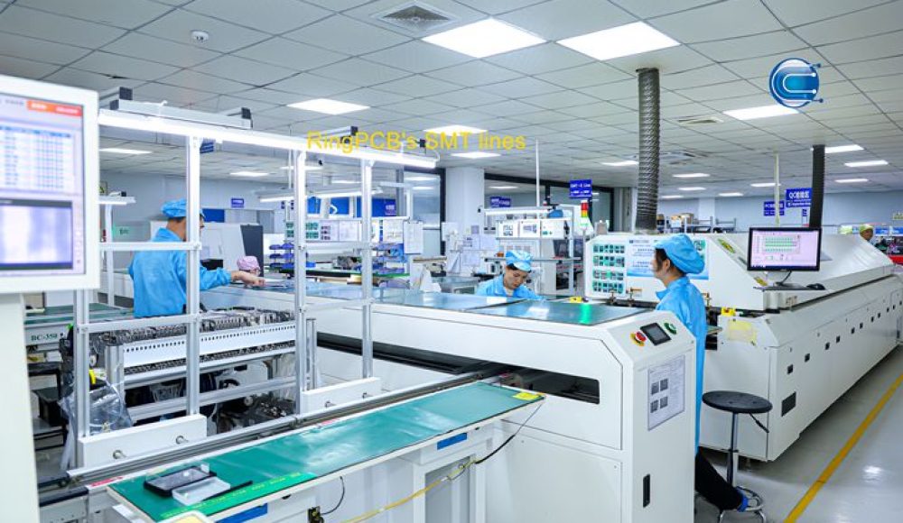
Every electronics project has different requirements at the prototype stage and mass production stage. Many engineers struggle with a common problem: a supplier that can build complex samples but fails to maintain stable yield once moving to volume production. At RingPCB, we separate our process specifications for Sample and MP (Mass Production) clearly, so you know exactly what can be achieved in R&D verification and consistent volume manufacturing.
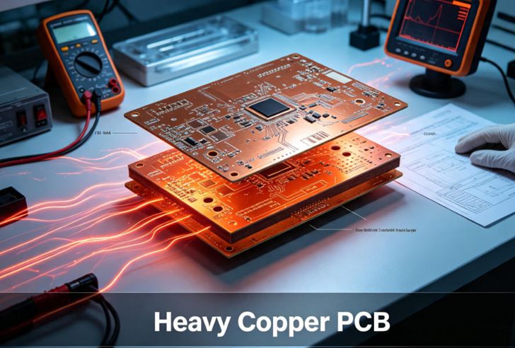
Our maximum layer count reaches 70 layers for samples and 30 layers for mass production. Board thickness ranges from 0.2 mm to 10 mm for samples, and 0.3 mm to 6.0 mm for mass production. We support ultra-fine trace & space: 2.0/2.0 mil (1/2 oz) for samples and 2.5/2.5 mil for mass production, plus 3.0/3.0 mil (1 oz outer layer) for samples and 4/4 mil for mass production. For heavy copper applications, we support up to 20 oz inner/outer copper for samples and 12 oz for mass production, ideal for high-current power boards.
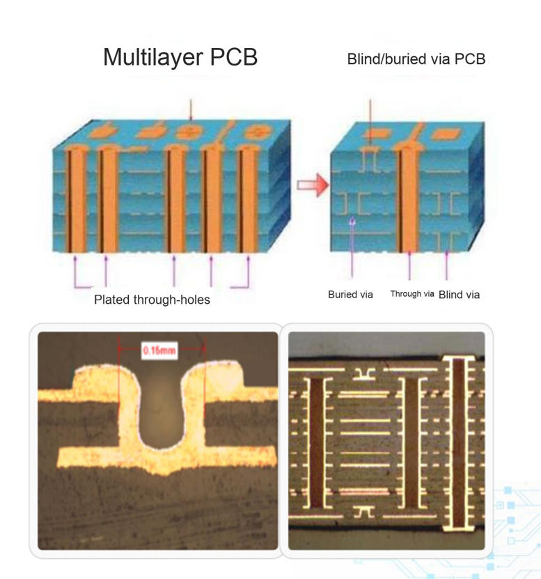
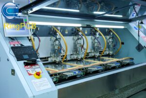
We offer flexible drilling options: mechanical holes down to 0.125 mm (sample) / 0.15 mm (MP), and laser microvias from 0.075 mm to 0.5 mm for samples. Our HDI capability covers 2+N+2 for mass production and ELIC for samples. Tolerance control is tighter for prototypes: impedance tolerance ±5% for samples vs ±10% for mass production, backdrill stub can be controlled as low as 0–8 mil for samples, and 8–16 mil for mass production.
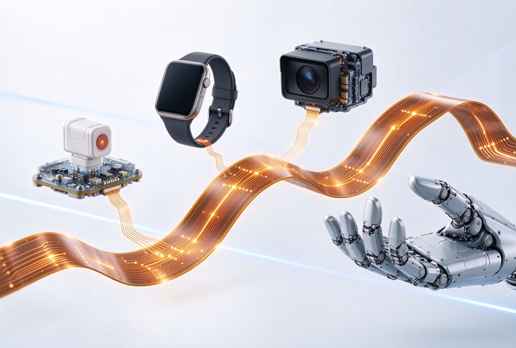
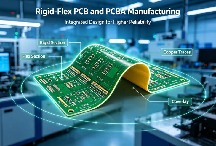
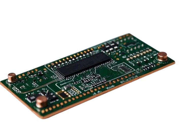
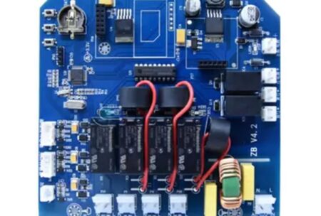
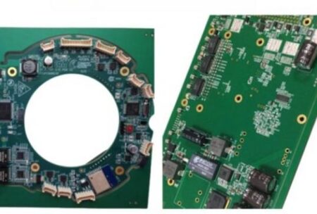
We work with well-known substrate brands including SYE, ITEQ, TUC, PANASONIC, Rogers, Taconic, ISOLA, Ventec, KB and HZ. Multiple surface finishes are available: ENIG, Immersion Tin, Immersion Silver, Plating Silver, OSP, OSP+ENIG, HASL (Pb & Pb-free), Gold Finger + ENIG and Hard Gold Plating. We manufacture a wide range of PCB types: high-layer boards, hybrid boards, heavy copper PCBs, copper-paste filled vias, stepped boards, gold finger boards, ATE boards, HDI, rigid-flex PCBs, embedded copper, embedded resistors, ceramic substrates and embedded capacitance/resistance boards.
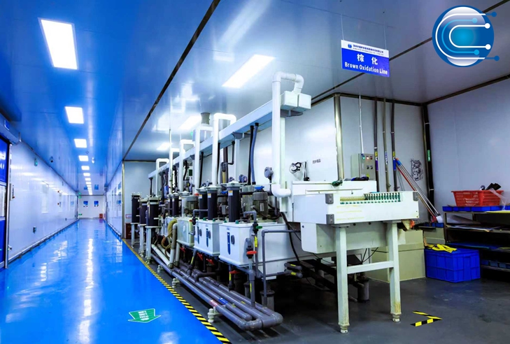
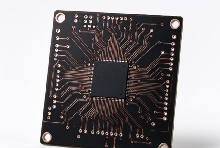
Beyond standard multilayer PCBs, we support special advanced processes: POFV plating over filled vias, drilled blind & buried vias, HDI microvias, backdrilling and edge plating. These advanced technologies solve pain points for high-speed signal integrity, dense BGA layouts and RF shielding.
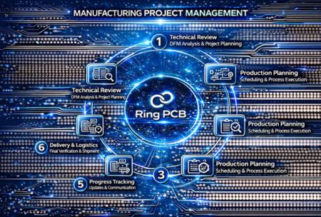
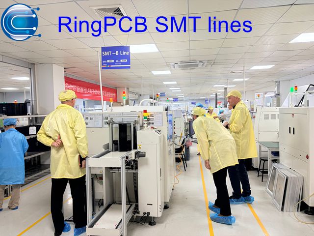
RingPCB provides fast 72-hour PCB prototyping and flexible small-batch orders, together with PCB assembly and component sourcing for full turnkey service.
We serve industrial control, communication, medical equipment, smart charging piles, collaborative robots, IoT and smart automotive industries. Note: We do not provide PCB design service. We manufacture PCBs based on your Gerber files and BOM.
Send your Gerber files and BOM to rfq@ringpcb.com for a technical review and quotation. www.ringpcb.com