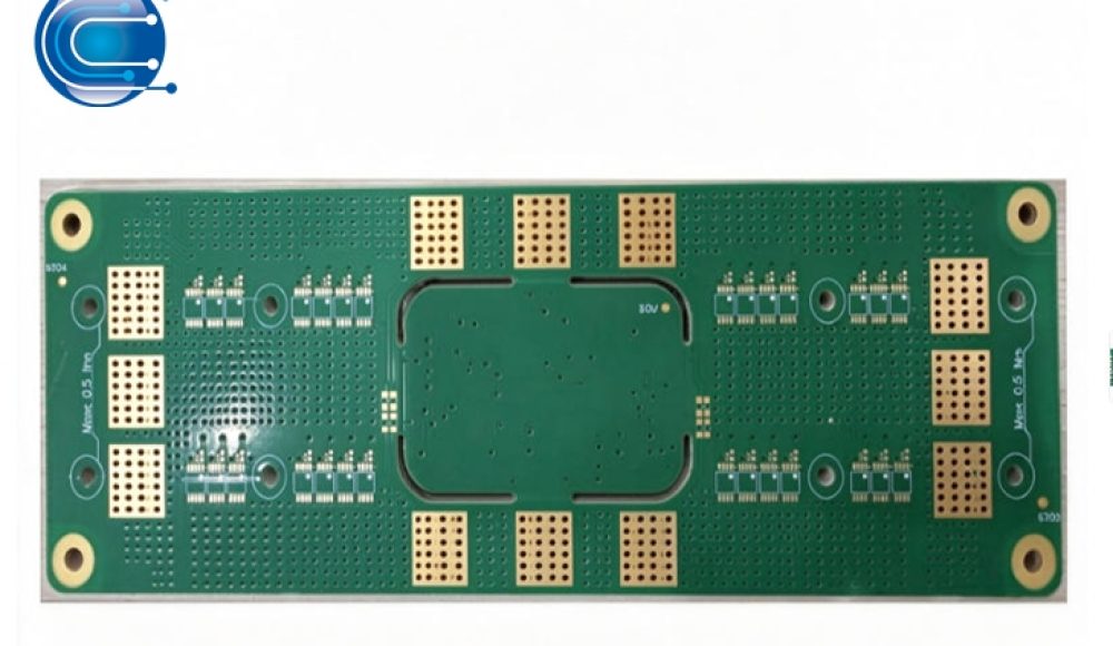
1. Why High Tg FR-4 and Heavy Copper Require Careful Manufacturing Control
Manufacturing a High Tg FR4 Heavy Copper PCB involves more than selecting a suitable laminate and increasing copper thickness.
Thicker copper changes the behavior of several fabrication processes, including circuit imaging, etching, lamination, drilling, plating and solder mask application. At the same time, High Tg FR-4 materials require appropriate lamination and thermal processing conditions to achieve the intended material performance.
When these technologies are combined, the manufacturer must coordinate material properties and process parameters throughout the PCB manufacturing workflow.
This is particularly important for industrial power boards, motor control circuits, power supplies and other products where electrical performance and long-term structural integrity are important.
2. Engineering Review: The First Step in Heavy Copper PCB Manufacturing
Before production begins, the manufacturer should review the complete fabrication package.
Important information includes:
- Gerber or ODB++ files
- Layer count and stackup
- Copper weight for individual layers
- Core and prepreg material specifications
- Finished board thickness
- Minimum trace width and spacing
- Drill sizes and plated-hole requirements
- Surface finish and solder mask specifications

This review helps identify potential conflicts between copper thickness, conductor geometry, material selection and manufacturing tolerances.
For example, a trace width suitable for a 1 oz copper layer may not be practical for a much thicker copper layer. The CAM team must consider etching compensation and the required finished conductor dimensions.
Early engineering review can prevent avoidable revisions after material preparation.
3. Circuit Imaging and Etching: Controlling Thick Copper Geometry
One of the most important challenges in Heavy Copper PCB manufacturing is maintaining conductor geometry during etching.
Why Thick Copper Is More Difficult to Etch
During the etching process, chemical solutions remove unwanted copper from the board. However, etching does not occur only vertically. The chemical process can also remove copper from the sides of the conductor.
This side etching is commonly described as undercut.
As copper thickness increases, greater etching depth and process compensation may be required. Excessive undercut can reduce the final conductor width and affect the electrical cross-section.
How Manufacturers Manage the Process
The manufacturer may need to adjust:
- Phototool artwork compensation
- Etching parameters and exposure time
- Conductor spacing
- Copper plating thickness
- Inspection criteria for finished traces
The required trace width and spacing should be determined according to the starting copper, final copper thickness and manufacturing process.
Heavy copper boards therefore need manufacturing-specific geometry review rather than simply reusing standard 1 oz PCB design rules.
4. Lamination: Managing Resin Flow Around Thick Copper
Lamination is another critical stage when manufacturing multilayer High Tg FR4 Heavy Copper PCBs.
During lamination, heat and pressure bond the PCB layers together through the resin system in the prepreg.
Thick copper features create greater differences in surface height. The spaces between conductors may also be deeper than those in conventional copper constructions.
If the selected prepreg does not provide sufficient resin flow and filling capability, potential manufacturing concerns include:
- Resin-starved areas
- Voids between copper features
- Localized delamination
- Inconsistent dielectric thickness
- Board warpage
Why High Tg FR-4 Material Compatibility Matters
High Tg FR-4 materials use resin systems formulated for particular thermal and mechanical properties.
The selected core and prepreg must be compatible with the required lamination cycle and the copper topography.
Manufacturers should evaluate resin content, glass fabric style, dielectric thickness, resin flow and the required press conditions.
Copper distribution also deserves attention. Large differences in copper coverage between layers can create uneven thermal and mechanical behavior during lamination.
A well-planned stackup should therefore consider both material properties and copper balance.
5. Drilling and Plated Through-Hole Reliability
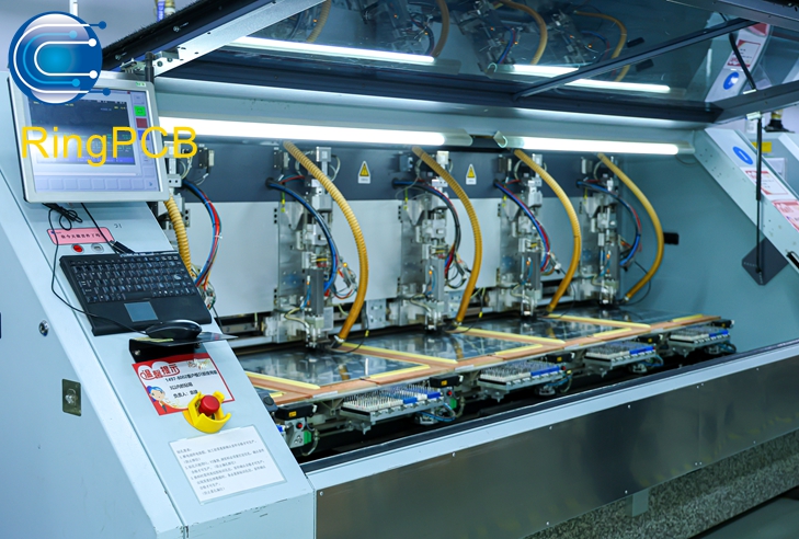
After lamination, mechanical drilling creates holes for component mounting and electrical interconnections.
For multilayer heavy copper boards, drilling quality is important because the holes must connect the specified copper layers through the board thickness.
Drilling Considerations
Thick copper and multilayer constructions can influence drilling conditions and hole-wall preparation.
The manufacturing team should review:
- Drill diameter and aspect ratio
- Finished hole size
- Board thickness
- Copper thickness at connected layers
- Drill tool selection and wear
- Hole-wall cleanliness
Drilling can generate resin smear on the hole wall. Desmear treatment is used to prepare the surface before copper plating.
Copper Plating
Electroless and electrolytic copper plating establish conductive connections through plated holes.
The required plating process must provide suitable electrical continuity and meet the specified hole-wall and finished-board requirements.
For power boards, via and plated-hole transitions deserve particular attention. A thick surface conductor cannot compensate for an inadequately specified or poorly manufactured interlayer connection.
The final acceptance requirements should be established in the fabrication drawing and procurement specification.
6. Solder Mask and Surface Finish on Heavy Copper Boards
Thick copper features create greater surface-height differences than standard copper constructions.
This can make solder mask application more challenging, particularly around conductor edges and raised copper features.
The manufacturer should review solder mask coverage, openings, clearances and the compatibility of the selected process with the board’s surface topography.
Surface finish selection also depends on the customer’s solderability, storage and assembly requirements.
For example, ENIG, immersion silver and lead-free HASL have different process characteristics. The appropriate finish should be selected according to component requirements, product specifications and manufacturing feasibility.
7. Inspection and Quality Control During PCB Manufacturing
High Tg FR4 Heavy Copper PCB manufacturing requires quality control at multiple stages.
A final electrical test alone cannot identify every process issue that may occur during fabrication.
Incoming Material Verification
Check laminate and copper foil specifications, material identification and relevant supplier documentation.
Inner-Layer AOI
Automated Optical Inspection helps identify opens, shorts and pattern defects before multilayer lamination.
Lamination and Microsection Evaluation
Where specified, cross-section analysis can help evaluate layer structure, dielectric conditions, plated-hole quality and copper thickness.
Electrical Testing
Continuity and isolation testing helps verify that the finished PCB meets the approved electrical netlist requirements.
Final Visual and Dimensional Inspection
Check board dimensions, surface conditions, solder mask, finished holes and other requirements specified in the fabrication drawing.
IPC-6012F provides qualification and performance requirements for rigid printed boards, while IPC-A-600 provides visual illustrations of acceptable and nonconforming conditions. The applicable acceptance class and requirements should be specified by the customer.
8. High Tg FR4 Heavy Copper PCB Manufacturing at Ring PCB
Ring PCB provides multilayer PCB manufacturing and Heavy Copper PCB fabrication for industrial electronics and power-related applications.
Established in 2008, the company operates a self-owned manufacturing facility of more than 10,000 square meters. Its published production capabilities include:
- Up to 30 layers for mass production
- Up to 70 layers for sample projects
- Inner and outer copper up to 12 oz for mass production
- Copper up to 20 oz for sample projects
- Finished board thickness up to 6.0 mm for mass production
- Finished board thickness up to 10 mm for sample projects

Ring PCB supports multilayer fabrication processes, including material preparation, lamination, drilling, copper plating, circuit formation, surface finishing and electrical inspection.
For High Tg FR-4 Heavy Copper PCB projects, the material grade, prepreg combination, copper distribution and manufacturing parameters are reviewed according to the actual board specifications.
Customers can submit Gerber files, stackup information and detailed technical requirements for manufacturing feasibility review.
If you need a PCB manufacturing partner for High Tg FR-4 or Heavy Copper PCB projects, contact rfq@ringpcb.com to discuss your requirements.
References
- HLCPCB. (2026). Heavy Copper PCB Manufacturing Supplier & Engineering Guide.
- Wrekin Circuits. How a PCB Is Made: Heavy Copper Manufacturing Considerations.
- IPC. (2023). IPC-6012F: Qualification and Performance Specification for Rigid Printed Boards.
- IPC. IPC-A-600: Acceptability of Printed Boards.